Table of Contents
In a world where gadgets merge intelligence with user experience, the integrated design project has become the beating heart of innovation. Imagine your smartwatch not only tracking steps but also seamlessly controlling your home lighting, health analytics, and even predictive scheduling.
That’s the promise and the challenge behind building the next generation of smart gadgets. In this article, we’ll walk through the concept, process, and real-world execution of integrated design projects, offering insights to creators, engineers, and tech enthusiasts alike.
What Is an “Integrated Design Project”?
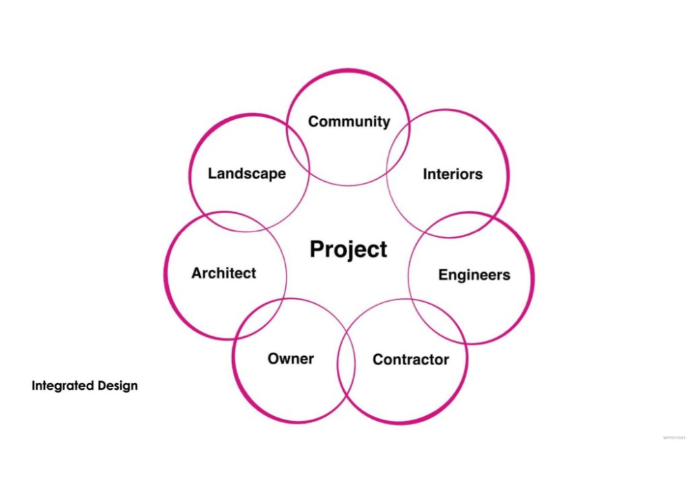
An integrated design project refers to a multidisciplinary effort that combines hardware, software, UX/UI, mechanical engineering, and systems thinking to deliver a cohesive, smart product. Rather than treating each component or domain in isolation, integration ensures all parts operate harmoniously.
Key Characteristics
- Cross-disciplinary collaboration: Teams of electrical, mechanical, firmware, and UX engineers must work hand in hand.
- Systems-level thinking: Designers consider how sensors, connectivity, battery, software, and interfaces relate.
- Iterative feedback loops: Prototyping, testing, and refining are continuous, not linear.
- Scalability and adaptability: The design must accommodate future features or new hardware modules.
Why Integrated Design Projects Are Crucial for Smart Gadgets
Avoiding Siloed Design Pitfalls
Designing hardware separately from software can cause compatibility issues, latency, or poor user experience. Imagine a beautifully engineered device whose software fails to maximize its sensors.
Boosting Innovation and Speed
When teams communicate early, you’ll uncover clever trade-offs like reducing sensor power or sharing physical components, accelerating development.
Enhancing User Experience (UX)
A truly smart gadget feels seamless. Integration ensures features like haptic feedback, adaptive UI, and sensor fusion happen intuitively.
Maintaining Competitive Edge
Brands that master integrated design can push boundaries with folding screens, advanced biometry, and AI-driven interfaces, and outpace competitors.
Core Phases of an Integrated Design Project
Below is a structured process many successful projects follow.
| Phase | Focus | Outcome |
| Concept & Requirements | Define user problems, market research | Feature list, viability analysis |
| System Architecture | High-level block diagrams | Modules, communication paths |
| Hardware & Mechanical Design | PCB layout, casing, thermal | Beta hardware prototypes |
| Firmware & Embedded Software | Drivers, RTOS, bootloader | Working firmware baseline |
| Connectivity & Integration | BLE, Wi-Fi, cloud APIs | Data pipelines, security |
| UX / UI Design | App, interface, user flows | Prototypes, wireframes |
| Testing & Validation | Functional, stress, compliance | Certification, QA |
| Manufacturing & Deployment | Supply chain, mass production | Product rollout, updates |
Each phase loops back; for instance, a UX test may force hardware adjustments. This iterative design is fundamental to integrated projects.
Essential Principles for Success
Start with Use Cases, Not Features
Before you decide on sensors or chips, sketch how users will interact with the gadget. What problems are you solving? Define primary and secondary use cases.
Modular Yet Unified Architecture
Design modular components (like sensor boards and communication modules), but maintain unifying standards (common buses, power rails, and protocols).
Co-design Hardware and Software
Don’t wait for the hardware to be “final” before starting software. Early simulation, FPGA models, or virtual sensors let software teams progress in parallel.
Emphasize Low Power Design
Smart gadgets often run on batteries. Use techniques like:
- Sensor fusion to avoid redundant sampling
- Duty cycling radios
- Dynamic voltage/frequency scaling
- Power gating of unused subsystems
Focus on Data Flow and Pipelines
From sensor acquisition to processing to user interface to cloud analytics, every step should be thought through for latency, accuracy, privacy, and security.
Build Testability In
Include:
- Test points for signals and power rails
- JTAG / SWD interfaces
- Self-tests and diagnostic modes in firmware
- Robust logging and remote diagnostics
Prioritize Security and Privacy
At the integrated-design level, security must be baked in, not bolted on:
- Secure boot and firmware authentication
- Encrypted communication (TLS, DTLS)
- Data anonymization and user consent policies
- Over-the-air (OTA) update capability
Document Everything
Rich architecture docs, interface definitions, version control logs, and traceability ensure new team members or partners can onboard quickly.
Technologies Driving Next-Gen Smart Gadgets
Sensor Fusion & Edge AI
Modern gadgets combine input from accelerometers, gyros, magnetometers, cameras, and more. Then, edge AI runs inference locally, reducing reliance on the cloud and improving responsiveness.
Low-Power Wireless Protocols
Protocols like Bluetooth Low Energy (BLE), Matter, Zigbee, and Thread enable gadget–hub–cloud interaction with minimal power draw.
Flexible and Printed Electronics
For wearables or embedded devices, printed sensors, flexible PCBs, and stretchable interfaces allow ultra-thin, conformable gadgets.
Energy Harvesting & Battery Tech
Integrating solar cells, piezoelectric elements, or thermal harvesters helps devices extend operational lifespan. Meanwhile, next-gen lithium polymer, solid-state, or micro-batteries reduce bulk.
Digital Twins & Simulation
Before physical prototyping, teams use digital twin models (thermal, mechanical, RF, and power) to simulate behavior. This catches design flaws early.
OTA & Edge Firmware Updates
An integrated design project ensures firmware can be updated securely post-launch, fixing bugs or enabling new features.
Case Study: Smart Health Wearable
Let’s illustrate with a fictional yet realistic example: a wearable that monitors hydration, heart rate variability (HRV), and sleep quality.
Defining Use Cases
- Hydration alerts: The device senses when the sweat rate is high and nudges the user to hydrate.
- Stress detection: HRV trends detect rising stress levels and suggest breathing exercises.
- Sleep coaching: Combines motion, heart rate, and skin temperature to guide better rest.
Architecture & Integration Decisions
- Sensor board: Includes ECG electrodes, accelerometer, temperature sensor, and sweat sensor.
- Processor: Ultra-low-power MCU with on-chip AI accelerator.
- Communications: BLE 5.2 + optional Wi-Fi.
- Power: 200 mAh battery, energy harvesting via motion or temperature gradient.
- Enclosure: Flexible strap, waterproof, ergonomic.
Co-design Highlights
- The firmware team began building sensor drivers and ML inference models in parallel with hardware development using simulation.
- The UX team tested the hydration reminder flow on a mobile app prototype; early feedback led to optimization of sensor placement and notification timing.
Testing & Iteration
- Thermal modeling flagged a hotspot near the sweat sensor; the layout was adjusted.
- Battery life proved short; sleep logic was reworked so only essential sensors ran in deep-sleep mode.
- Connectivity failure during high motion spurred fallback data caching logic.
Launch & Updates
- The device passed regulatory compliance (e.g., FCC, CE).
- The OTA update allowed adding the ECG waveform visualizer and new algorithms post-release.
This integrated design project delivered a cohesive, effective smart wearable.
Conclusion
An integrated design project is not merely about building a smart gadget; it’s about unifying interdisciplinary expertise into a single, coherent vision. When hardware engineers, software developers, UX designers, and system architects collaborate from day one, the outcome is more robust, scalable, and delightful to the user.
If you’re embarking on building the next generation of smart gadgets, lean into systems thinking, iterate early, and always think about the user’s journey. With good planning, a modular yet unified architecture, and attentive testing, your integrated design project can become the next breakthrough device.
Ready to start your project? Define your use cases, gather your cross-disciplinary team, and begin sketching your system architecture today.
Frequently Asked Questions (FAQs)
Q1: How does an integrated design project differ from traditional product development?
In traditional development, hardware, firmware, and UX often work in silos and pass a design baton between teams. An integrated design project aligns all disciplines from the start, enabling better trade-offs, fewer mismatches, and more seamless user experiences.
Q2: What challenges do teams often face in integrated design, and how can they overcome them?
Common challenges include cross-team miscommunication, scope creep, and debugging across domains. Effective solutions are regular syncs, feature freeze policies, modular logging, and early prototyping.
Q3: Can small startups use integrated design approaches?
Absolutely. In fact, smaller teams may have an advantage in shorter communication paths and more flexibility. Use agile iterations, shared tools, and open standards to manage complexity.
Q4: How important is power optimization in integrated smart gadget design?
Very important. Battery life is often a key competitive factor. Techniques like sensor fusion, duty cycling, dynamic voltage scaling, and power gating are essential in integrated projects.
Q5: After product launch, how do integrated design projects evolve?
They evolve through OTA firmware updates, data-driven feature additions, hardware revisions, and modular upgrades. A strong foundational architecture makes this evolution smoother.

It’s fascinating how gaming platforms are prioritizing responsible play now – deposit limits & verification are key! Seeing 88 lucky ph legit focus on security is a smart move for both players & the industry. It builds trust! 🤔
Solid analysis! Seeing responsible gaming features like deposit limits at 88 lucky ph casino is great. It’s key for long-term enjoyment & smart betting – a good sign of a regulated platform! 👍
Interesting read! Seeing more platforms prioritize responsible gaming – the deposit limits at 88 lucky ph game sound smart. Transparency & security are key, especially with online slots! 👍